Memories,. food for the EGO.
Manifestation
of memories into self-esteem, honor, dignity and many other traits characterize
the individual. Obviously, memories
are stored in the brain and scientist have identified, subdivided, labeled
and compartmentalized the brain in many functional regions. Computer memory like human memory manifests
it presents in different ways to perform a variety of functions; and computer
memory has been divided into partitions, subsystems and specialization. Although
the memory in today's computers have not been programmed with
personality traits, some PC systems do demonstrate personality disorders,
particularly the one this article was written with.
There
is an abundance of terms that have been used to describe or label computer
memory functions, features and attributes. Some terms apply to the hardware
technology, some terms apply to the packing of these chips and others apply
to the memory usage or memory systems within the computer. Collectively,
all of these terms may be confusing and to help sort out and clarify these
labels we will look at how these items have been applied to computer memory. To
simplify this task, the effort will be divided into the following 5 areas:
packing, parity & ECC, buffered/non-buffered, systems and labels.
MEMORY PACKAGING
Just as memory
technology has evolved so has memory packaging. Shown below is a table of the different
form factors (packaging) that has been used in memory deployment over the
past 25 years.
|
PINS |
Package Type |
Description |
Commonly
Found In |
|
22
30
72
72
100
144
144
168
184
184
200 |
DIP
SIMM
SIMM
SODIMM
DIMM
SODIMM
MICRODIMM
DIMM
RIMM
DIMM DDR
SODIMM |
Dual In-line Package
Single In-line Memory Module
Single In-line Memory Module
Small Outline DIMM
Dual In-line Memory Module
Small Outline DIMM
Micro DIMM
Dual In-line Memory Module
Rambus In-line Memory Module
Dual In-line Memory Module
Small Outline DIMM |
Early computers 8080, 8086
Early computers 386, 486
486, early Pentium
Laptop computers
Printers
Laptops
Sub-Notebooks
Current desktops P2, P3, P4
Current desktops P3, P4
Current desktops P4
Laptop computers |
Besides the
pin count, other obvious marking will be the number and positioning of the
notches along the bottom of the memory module. These notches help correctly
orientate the proper RAM module or prevent the installation of an incorrect
memory type by blocking any memory module that does not have the correct
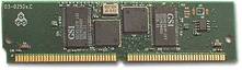
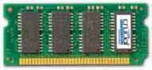
notch arrangement. The following images will help identify the packaging
type.
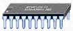
16-20 pin DIP
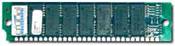
30 pin SIMM
72 pin SIMM
72 pin SODIMM
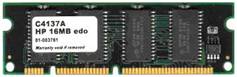
100 pin DIMM / SODIMM
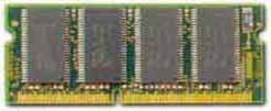
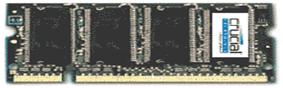
144 pin SODIMM
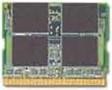
144 pin MICRODIMM
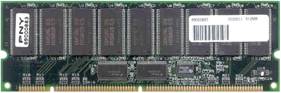
168 pin DIMM
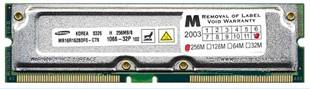
184 pin RIMM
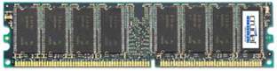
184 pin DIMM DDR
200 pin SODIMM
PARITY & ECC
Parity and
ECC (Error Correction Code) are different forms of data quality monitoring
and error detection & correction. Initially, memory modules came in two
types, parity and non-parity and later this evolved into ECC.
Non-parity memory contains one bit of memory
for every bit of data to be stored. Normally there are 8 bits of data for
each byte of memory. Non-parity memory provides no error detection capabilities
at all.
Parity checking is a rudimentary method
of detecting simple, single-bit errors. It was first used on the original
IBM PC in 1981 and has been used in every PC until the early 1990s. Parity
memory adds an extra bit for every eight bits of data; therefore 9 bits of
data are used to store each byte.
When parity
checking is enabled a logic circuit called a parity generator/checker examines
each byte written to memory and determines whether the data byte has an even
or an odd number of ones. If there is an even number of ones, the ninth (parity)
bit is set to 1; otherwise if there is an odd number
of ones then it is set to 0. The result is that no matter how many ones there
were in the original eight data bits, there will be odd number of ones when
you look at all nine bits together. This is called odd-parity and
it is also possible to have even-parity,
where the generator makes the sum come out even. The standard is odd parity.
The following table shows an example of how odd-parity and even-parity work.
|
Sample byte with 8 data bits |
# of '1s' in sample byte |
Odd
Parity |
Even
Parity |
|
Parity
Bit |
# of '1s' in sample byte with parity bit |
Final
sample stored with parity bit |
Parity
Bit |
# of '1s' in sample byte with parity bit |
Final
sample stored with parity
bit |
|
00000000 |
0 |
1 |
1 |
00000000
1 |
0 |
0 |
00000000
0 |
|
10110011 |
5 |
0 |
5 |
10110011
0 |
1 |
6 |
10110011
1 |
|
00100100 |
2 |
1 |
3 |
00100100
1 |
0 |
2 |
00100100
0 |
|
11111111 |
8 |
1 |
9 |
11111111
1 |
0 |
8 |
11111111
0 |
Parity
checking is not perfect nor does it protect against double-bit errors. A
double-bit error is where 2 bits in the same byte have changed. For example,
say the data byte 00100100 is read and stored as "00100100 1" including
the parity bit. Then let's say the byte is read back as "01100000 1".
Here, there are two bits that have flipped, one of them from 1 to 0 and the
other from 0 to 1. But the total number of 1s is still odd. Fortunately,
the odds of encountering a single bit error are small and the odds of encountering
a double-bit error are extremely rare.
ECC (Error Correction Code) was also
known as Error Correcting Circuits or Error Correcting Code is an advanced
error detection and correction protocol developed to overcome the shortcomings
of parity memory. This protocol detects both single-bit and multi-bit errors
and it will correct single-bit errors on the fly and flag the operating system
of a multiple bit error.
ECC
uses a special algorithm to encode information
in a block of bits. This block
contains adequate detail information
to recovery a single bit error. Instead of using 1 bit to protect an 8 bit
word, ECC uses 7 bits to protect 32 bits of data or 8 bits to protect 64
bits of data.
ECC
will work with standard parity memory modules as well. Since parity DIMMs (Dual
Inline Memory Module) are 72 bits wide this means that there is 1 bit for
every 8 bits of data; thus, 64 bits of data has 8 bits available for parity
that can be used by the ECC system. A parity SIMM
(Single Inline Memory Module) is 36 bits wide, 32 bit for data and 4 bits
for parity. Thus, if two modules
were used then you would have 2 x 32 = 64 bits of data and 2 x 4 = 8 parity
bits that can be used by the ECC system.
The difference
between the parity memory and ECC memory is that parity memory will work
in both modes. However, ECC memory
only works in ECC mode. ECC modules contain one extra bit per byte like the
parity memory; however, the extra bites cannot be individually accessed which
is required for parity operation.
BUFFERED/NON-BUFFERED
Most of the specifications related to
memory type depend on the system board design. This is also the case with
Buffered and Non-Buffered DIMM. A buffer is a driver. Some system boards
include drivers for the memory control signals, while others rely on the
memory module to drive its own memory control signals. A buffered module
has drivers on it; a non-buffered module does not. A system that requires
buffered modules will not function with a non-buffered module and vise versa
When a computer first boots one of the
initializations tasks is POST (Power On Self Test).
During this process the computer detects all of the attached hardware, like
processor, RAM, keyboard, mouse and many other components. With
DIMM ram it needs to detect the configuration of the memory module in order
to properly interface with it. On
a buffered DIMM, there is a small EPROM called SPD (Serial Presence Detect)
that stores information abut the module. The
computer reads this information
and will know what kind of RAM is installed and how to interface with it.
MEMORY SYSTEMS
Memory is not storage; although data stored on a disk can be stored in memory.
Storage is not memory; although data in memory can be stored on a disk.
Memory can be storage if the data is stored in a Read Only Memory (ROM)
In
the early days of computer development the above distinction was not as clear
as it is today. Over the years the data stream between the processor and
storage has lengthen considerably. Now
instead of going straight from storage to processor it is not uncommon for
data to go through several memory holding locations. The
data flow in today's computers may go from the hard drive to a hard drive cache, then to main memory, then to L2 cache, then to L1 cache, then to CPU registers where
it would be evaluated or executed-on by the processor and then end up in
a video memory or possibly a printer
or modem buffer or even back to the hard drive. All of these are memory
systems and the following will describe their application.
Hard Drive Cache is a small
cache integrated into the hard drive circuitry that provides a data buffer
between the operating system data read/write requests. The cache helps
prevents the overflow of data to or from the operating system.
Main Memory is the primary RAM of a computer. This is where all programs and data are
loaded when a software application is launched provided the RAM size is adequate
to hold all of the data. Obviously, RAM is much faster than a hard driver
therefore; RAM serves as a fast data pool for the processor.
L3 Cache is extra cache that sits on the system
board between the processor and main memory for processors that already contain
L1 and L2 cache. L3 performs the same function as L2 cache except in a higher
volume capacity.
L2 Cache is a smaller
amount of SRAM than L3 and is located between the L1 cache and L3 cache
or main memory. L2 cache has
the same purpose as L1 cache and depending on the processor it may or may
not integrated into the processor die. L1 Cache is a smaller amount
of SRAM memory used as a cache that is integrated or packaged within the
same module as the processor. It is located between the CPU registers and
the L2 cache. The L1 cache is clocked at the same speed of the processor
and provides very fast access to the most recently used data. L1 cache
is used to temporarily store instructions and data, making sure the processor
has a steady supply of data to process while the main memory fetches and
makes available new data. The
L1 cache checks the L2 cache before going to main memory.
CPU Register is a very small amount of memory
located between the L1 cache and the ALU (Arithmetic Logic Unit) or the CU
(Control Unit) of the processor. The
register holds the individual bytes of data that are required for the ALU
execution.
There are
a couple more memory systems with indirect flow of data to the processor. One major system is hardware BIOS (Basis Input Output System) which is a flash ROM or EEPROM chip
that contains all program instructions for the operating system to access
the respective hardware features. BIOS is found on a system board, video
card, audio card, SCSI card, network card, hard drives, zip drives and CD/DVD
drives and any other card plugged or connected into the motherboard. You will also have, but may not notice
the BIOS for your modem, printer, keyboard, video camera, scanner or any
other hardware that is plugged into you system particularly if it is PNP
(Plug and Play) compliant.
CMOS Memory (Complementary Metal-Oxide Semiconductor) also
known as CMOS RAM is where personal
system board settings are retained. Originally, CMOS held the type of hard
drive that was connected to the motherboard so the system would not have
to re-detect it every time it was booted. As system boards and peripheral equipment
become more advanced the CMOS has grown in size and has become the home for
all personalized system board setting.
Virtual memory is the page file system (swap file)
which is located on the hard drive. This
is a temporary holding location of data that is paged from the RAM to the
hard drive. When the operating system is shut down this data is lost.
Tag memory, TAG memory
acts as an index for the information
stored in L2 cache. It is usually composed of SRAM.
Video Memory is where the data bytes are located
that are used to update the screen image by way of the RAMDAC (Random Access
Memory Digital Analog Converter).
Printer or Modem buffer is a small
cache integrated into the circuitry that provides a data buffer between
the system read/write data requests. The cache helps prevents the overflow
of data to or from the system.
MEMORY LABLES
There are
a couple of data labels that need to be addressed and the following data
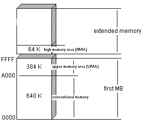
labels only apply to the main memory of the computer. Conventional Memory and Upper
Memory subdivide the first 1 meg of memory. Expanded
Memory and Extended Memory apply
to any memory above the first 1 meg. Finally, Upper
Memory is a small segment of memory above the first 1 meg.
Conventional Memory is the first 640 Kilobytes of main
memory. This is where most all
DOS programs run.
Upper Memory is the 384 Kilobytes of main memory
immediately above the 640 Kilobytes.
Expanded Memory is all memory above the first 1 meg that is addressable by 8086 and 8088 processors.
Extended Memory is all memory above the first 1 meg that is addressable by 80286 and greater processors.
High Memory is the first 64 Kilobytes of Extended
Memory.
NEXT MONTH
In part 3 of this series we will look at current R&D memory
technology and examine some of the technologies that may create the next
generation of memory modules. An
addendum, (Part 4) will be added to this series dedicated exclusively to
memory sizing and performance.
REFERENCES
- Glossary
of Memory Terms http://www.crucial.com/library
- Computer Memory, . http://home.cfl.rr.com/bjp/
Click here to download a pdf
version of the April Baby Steps to the
Future column.
|